SK hynix Indiana Groundbreaking: Bringing Next-Generation AI Memory to the U.S.

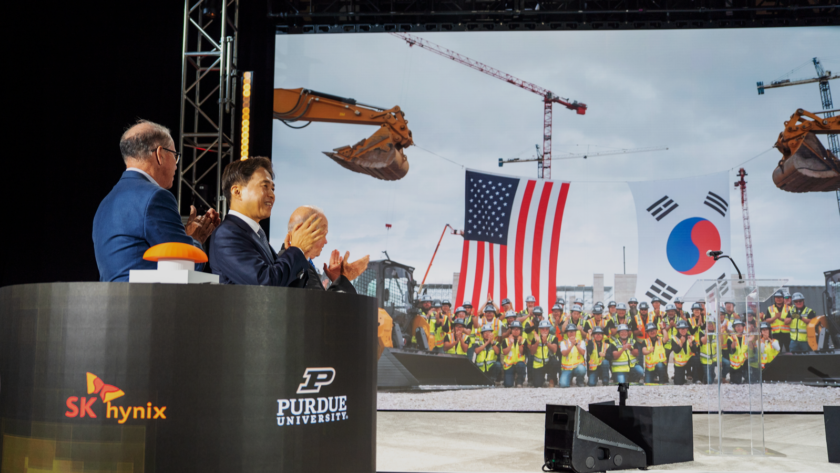
SK hynix's recent groundbreaking ceremony in West Lafayette, Ind., marked a major milestone in development of the U.S. semiconductor supply chain. The project – an investment of more than $4 billion – will establish the company's first high-bandwidth memory (HBM) production facility in the U.S. and position Indiana as a hub for AI innovation.
HBM has become a critical enabler of AI systems because it can rapidly transfer the massive amounts of data required for large language models. The Indiana facility will include an advanced packaging production line and an R&D testbed. Its cleanroom is scheduled to open by October 2028 with mass production of "Made in the USA" HBM planned for the second half of 2029.
The Indiana facility is another example of the strong economic partnership between the U.S. and Korea. Cutting-edge wafers produced by SK hynix in Korea will be sent to Indiana for advanced packaging and testing before reaching U.S. customers.
The groundbreaking ceremony was held August 27 on the Purdue University campus and drew prominent leaders from both nations, including U.S. Senator Todd Young, Indiana Governor Mike Braun, Purdue University President Mitch Daniels, and Kang Kyung-wha, Ambassador of South Korea to the U.S.
The Indiana facility is expected to create approximately 7,000 direct and indirect jobs during construction and commercial operations. More than 100 suppliers will support the fab's material, component, and equipment needs. During the ceremony, SK hynix also signed a memorandum of understanding with Purdue University for research and development in advanced packaging technology.
For a detailed overview of the groundbreaking, its significance for the U.S. and Indiana, check out the links below:
- Story: SK hynix Indiana fab breaks ground as new hub for U.S. AI innovation
- Press Release: SK hynix Holds Groundbreaking Ceremony for HBM Production Base in Indiana, “Beginning a New Future for US-Korea AI”
- Full Event Video: SK hynix Indiana Fab Groundbreaking Ceremony