Absolics: How Glass Substrates Are Powering the AI Revolution

- Georgia United States
From powering software applications to fueling platforms such as ChatGPT, artificial intelligence (AI) is playing a more visible role in people’s daily lives. As this AI revolution unfolds with many opportunities for technological advancement, it also brings some challenges – including the significant amount of energy that AI requires to operate. Goldman Sachs forecasts that AI-driven power consumption could reach over 1,000 terawatt-hours by 2030 – nearly double the amount of power generated by South Korea for the whole of 2022.
To help solve this challenge, SK companies are advancing more efficient solutions and materials that meet the growing demand for AI and form integral foundations for electronic devices. One of these materials is glass substrates, thin layers of glass on which processing and memory chips can be mounted together to create the brains of a computing system.
Manufactured by Absolics, a U.S.-based SK company, glass substrates leverage thermally stable technology and can hold more chips and enable larger packages. Along with other special design and manufacturing capabilities, their technology can significantly improve power consumption and data speed – including up to a 50% reduction in power consumption and a 30% improvement in signal performance, among other benefits.
Key advantages for AI usage
As AI platforms and Large Language Models (LLMs) become more sophisticated, Absolics anticipates launching high-volume manufacturing of its glass substrates in 2025. These substrates can support high-performance computing for AI platforms thanks to three key advantages: smooth surfaces, thermal resistance, and space efficiency.
Smooth surfaces allow for more precise circuit implementations and better chip-to-chip connections, which improve power efficiency and reduce electrical signal loss. The substrates’ thermal resistance results in less distortion under heat, leading to enhanced packaging density that’s well-suited for precision semiconductors such as High Bandwidth Memory (HBM), used in tandem with graphic processing units (GPUs) to power leading AI functions.
Additionally, one of Absolics’ key element technologies is the active/passive parts embedding in the glass core. This makes routing much more efficient than conventional designs by embedding multilayer ceramic capacitors (MLCCs) directly into the package substrate instead of using the surface-mounting technology that conventional organic substrates require. This reduction in routing drives greater space efficiency to allow for more compact designs and better utilization of limited space. It also provides extra surface space for additional XPUs and memory, supporting a more power-efficient performance.
Ultimately, these key advantages contribute to glass substrates’ enhanced package performance in terms of signal/power integrity, and design scalability.
The top markets for glass substrates
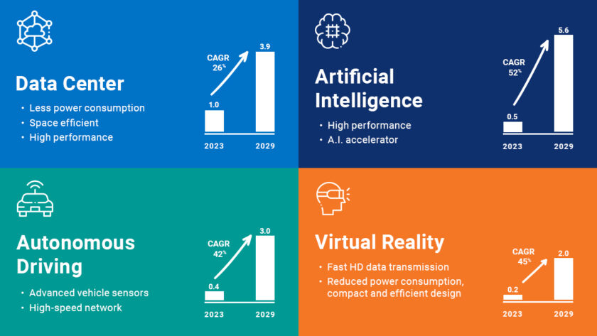
As AI technology continues to expand, so does the demand for high-performance computing that can quickly process large volumes of data. Advanced semiconductor packages using glass substrates will enhance high-performance computing and broaden their end markets to include AI servers, data centers, virtual reality, 5G, satellite communications, network infrastructure, autonomous vehicles, and more.
Absolics is developing a strong and resilient supply chain to serve these industries.
A major player in U.S. and global markets
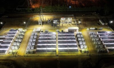
Absolics – which has heavily invested into its Covington, Georgia facility – aims to establish a novel ecosystem in advanced packaging to support the growth of the high-performance compute and AI markets and meet the demand here in the U.S. and abroad.
Absolics’ innovative solutions and manufacturing processes for glass substrates serve as a prime example of how SK is advancing high technology. From investing in key U.S. markets to developing critical technology that will power AI platforms, SK is driving toward a stronger future – and it all starts with innovation today.